ProPOV Day 3
18 May 2011
Today was day three of the ProPOV build. I spent the whole day printing, transferring, and etching circuit boards.
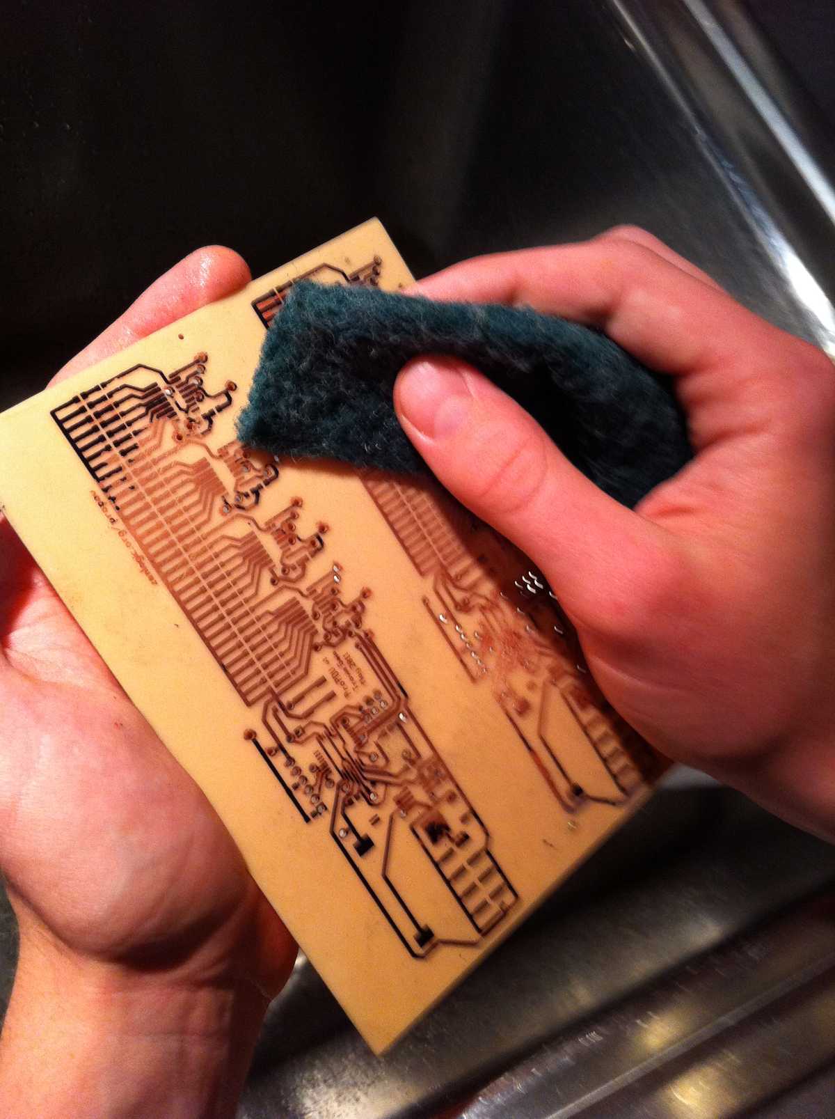
I use the toner transfer method of etching, which means I print the design on a laser printer and melt the toner from the printed design onto the copper-clad PCB. I have used a clothes iron to facilitate the transfer, but LVL1 has a modified personal laminator that applies nicely even pressure and heat.
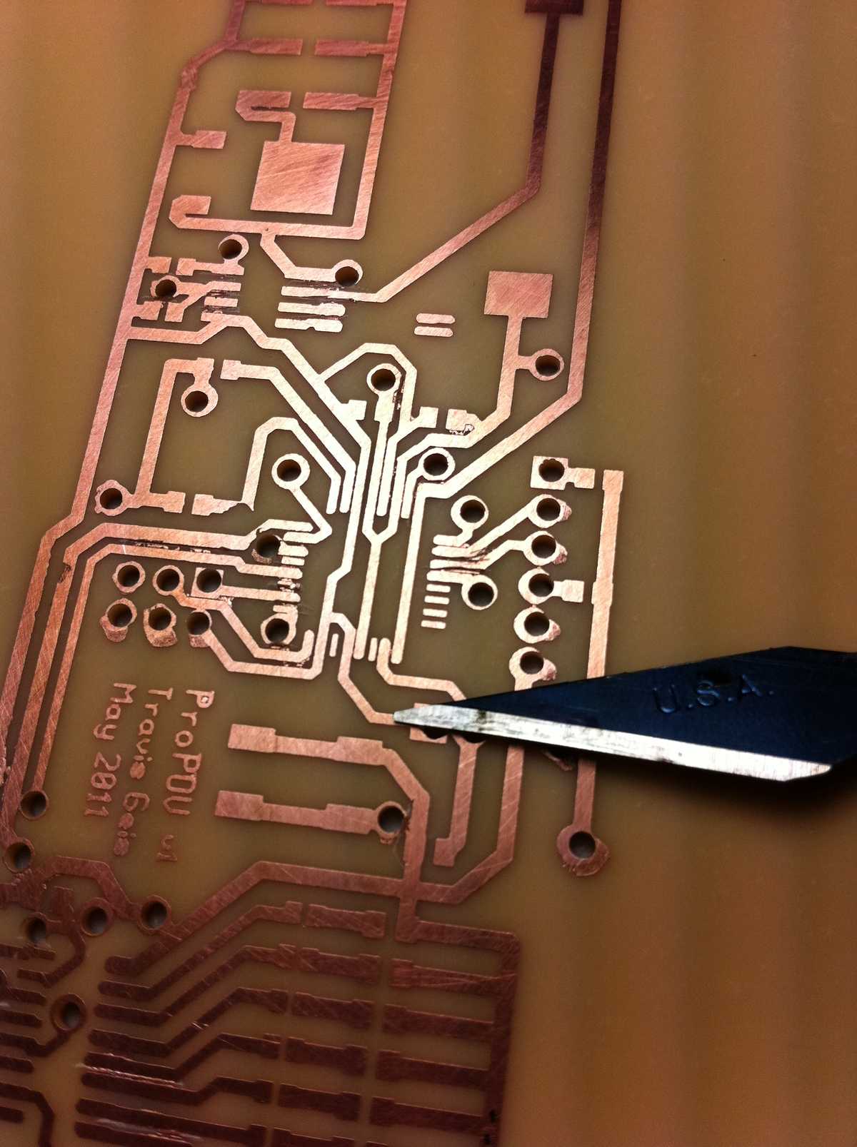
The toner transfer was mostly successful. I managed to etch four of six boards I transferred, and the two failures were relatively minor. Tinning the boards involved painting them thoroughly with flux, and melting solder onto the pads and vias. The vias, places where the traces switches sides on the board, need to conduct through the thickness of the board.
Originally, I intended to melt a large blob of solder onto the vias, and hope it tinned through to the other side. However, the solder beaded up on the iron and the hot side of the board, and so I had to construct my vias with a wire running through the holes on the board. The through-hole wire method takes inordinate amounts of time for relatively few vias, so I hope to pursue better options in the future.


